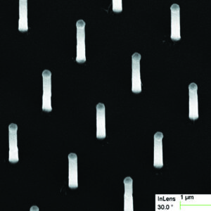
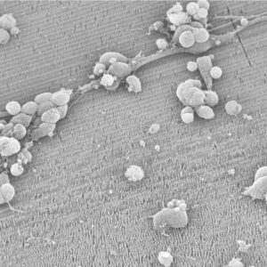
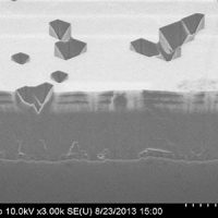
It’s fascinating to learn how the laws of Physics vary from the macroscopic world to the microscopic world. Some of the physical properties that we often ignore in macroscale become significant in nanoscale, while a few other properties become less noticeable in nanoscale but are highly crucial in macroscale. Synthesizing, manipulating, and analyzing nanomaterials using advanced technologies open a wide range of opportunities to seek answers to some of the fundamental scientific questions. The challenges remain how to synthesize functional nanomaterials, their assembly, patterning, and their applications for the betterness of science and society.
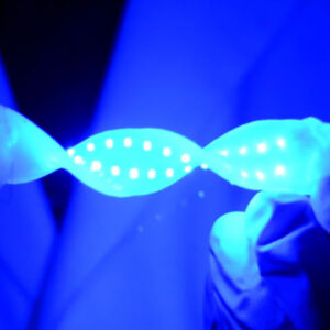
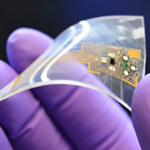
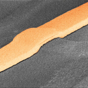
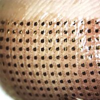
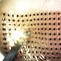
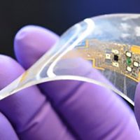
On the other hand, we are going through a transition period from rigid electronics to flexible and soft electronics. And, this transition demands new types of materials than that of conventional electronics. For example, silicon (Si) is one of the primary materials in modern electronics, which is rigid. However, emerging soft devices explore flexible and soft materials such as polyimide or silicones. Transitioning from rigid materials to flexible and soft materials open a wide range of potential materials because of the vast world of natural and artificial polymers. Also, the mechanical flexibility and stretchability can be achieved using rigid materials based on geometric patterns and mechanics of thin films. These issues of selecting materials for emerging devices require fundamental studies of materials properties, their limitations, and their benefits of using in the devices.
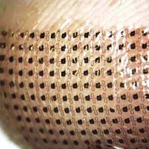
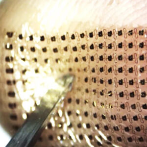
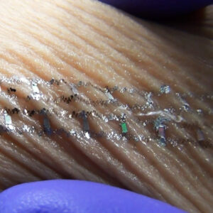
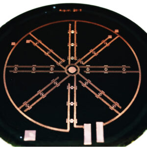
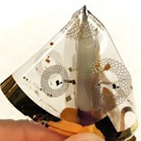
The other paramount concern of the emerging flexible and soft devices is reliable manufacturing. Currently, there exists no universal manufacturing process to realize soft electronics when compared with the rigid printed circuit boards (PCB) technology. Moreover, the integration density and complexity of the demonstrated soft and stretchable devices remain far behind conventional electronics. To exercise the full benefits of this emerging technology for real-life applications, the technology must be matured and reliable and need to be compatible with industrial manufacturing. The big question is- how to engineer a universal manufacturing method that is compatible with the industrial production of highly integrated soft electronics! Can we devise a stretchable printed circuit board (SPCB) technology? Is it possible to engineer a hybrid technology that will use existing rigid surface mount devices (SMD) in soft and stretchable circuits?
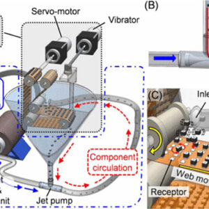
The additional manufacturing problem is the assembly of the components in the soft circuits and their packaging. Conventional robotic pick-and-place machines are mostly limited to assemble components onto rigid substrates. Their yield is also low when the dimensions of the chips or dies become microscopic. Is it possible to engineer a self-assembly technique that can overcome many of these limitations- can assemble microscopic components with high yield regardless of the mechanical properties of the substrates?
It’s fascinating to learn how the laws of Physics vary from the macroscopic world to the microscopic world. Some of the physical properties that we often ignore in macroscale become significant in nanoscale, while a few other properties become less noticeable in nanoscale but are highly crucial in macroscale. Synthesizing, manipulating, and analyzing nanomaterials using advanced technologies open a wide range of opportunities to seek answers to some of the fundamental scientific questions. The challenges remain how to synthesize functional nanomaterials, their assembly, patterning, and their applications for the betterness of science and society.
On the other hand, we are going through a transition period from rigid electronics to flexible and soft electronics. And, this transition demands new types of materials than that of conventional electronics. For example, silicon (Si) is one of the primary materials in modern electronics, which is rigid. However, emerging soft devices explore flexible and soft materials such as polyimide or silicones. Transitioning from rigid materials to flexible and soft materials open a wide range of potential materials because of the vast world of natural and artificial polymers. Also, the mechanical flexibility and stretchability can be achieved using rigid materials based on geometric patterns and mechanics of thin films. These issues of selecting materials for emerging devices require fundamental studies of materials properties, their limitations, and their benefits of using in the devices.
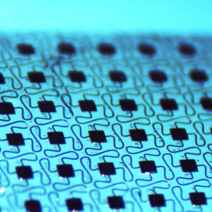
The other paramount concern of the emerging flexible and soft devices is reliable manufacturing. Currently, there exists no universal manufacturing process to realize soft electronics when compared with the rigid printed circuit boards (PCB) technology. Moreover, the integration density and complexity of the demonstrated soft and stretchable devices remain far behind conventional electronics. To exercise the full benefits of this emerging technology for real-life applications, the technology must be matured and reliable and need to be compatible with industrial manufacturing. The big question is- how to engineer a universal manufacturing method that is compatible with the industrial production of highly integrated soft electronics! Can we devise a stretchable printed circuit board (SPCB) technology? Is it possible to engineer a hybrid technology that will use existing rigid surface mount devices (SMD) in soft and stretchable circuits?
The additional manufacturing problem is the assembly of the components in the soft circuits and their packaging. Conventional robotic pick-and-place machines are mostly limited to assemble components onto rigid substrates. Their yield is also low when the dimensions of the chips or dies become microscopic. Is it possible to engineer a self-assembly technique that can overcome many of these limitations- can assemble microscopic components with high yield regardless of the mechanical properties of the substrates?
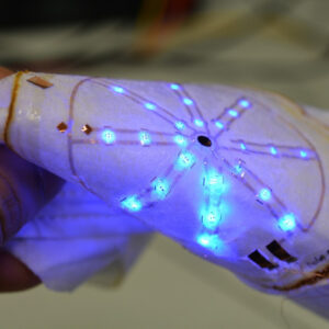
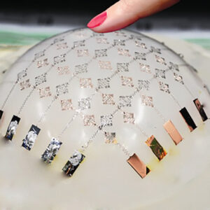
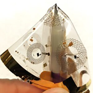
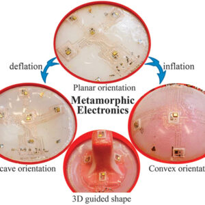
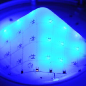
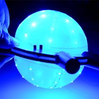
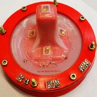
Finally, this emerging technology enables a new era of electronics where the devices can be shape-adaptive, can be “Metamorphic”. Developing such electronics requires designing devices that can sustain different strain at different locations on its surface to accommodate desire shapes. Such metamorphic electronic systems with integrated functionalities that can achieve many other shapes than just sphere. Once fully developed, most electronic systems known to humankind could morph to take on new exciting form factors. We could demonstrate many fascinating shape-adaptive devices and functions. Imagination is limitless!